Table Of Content

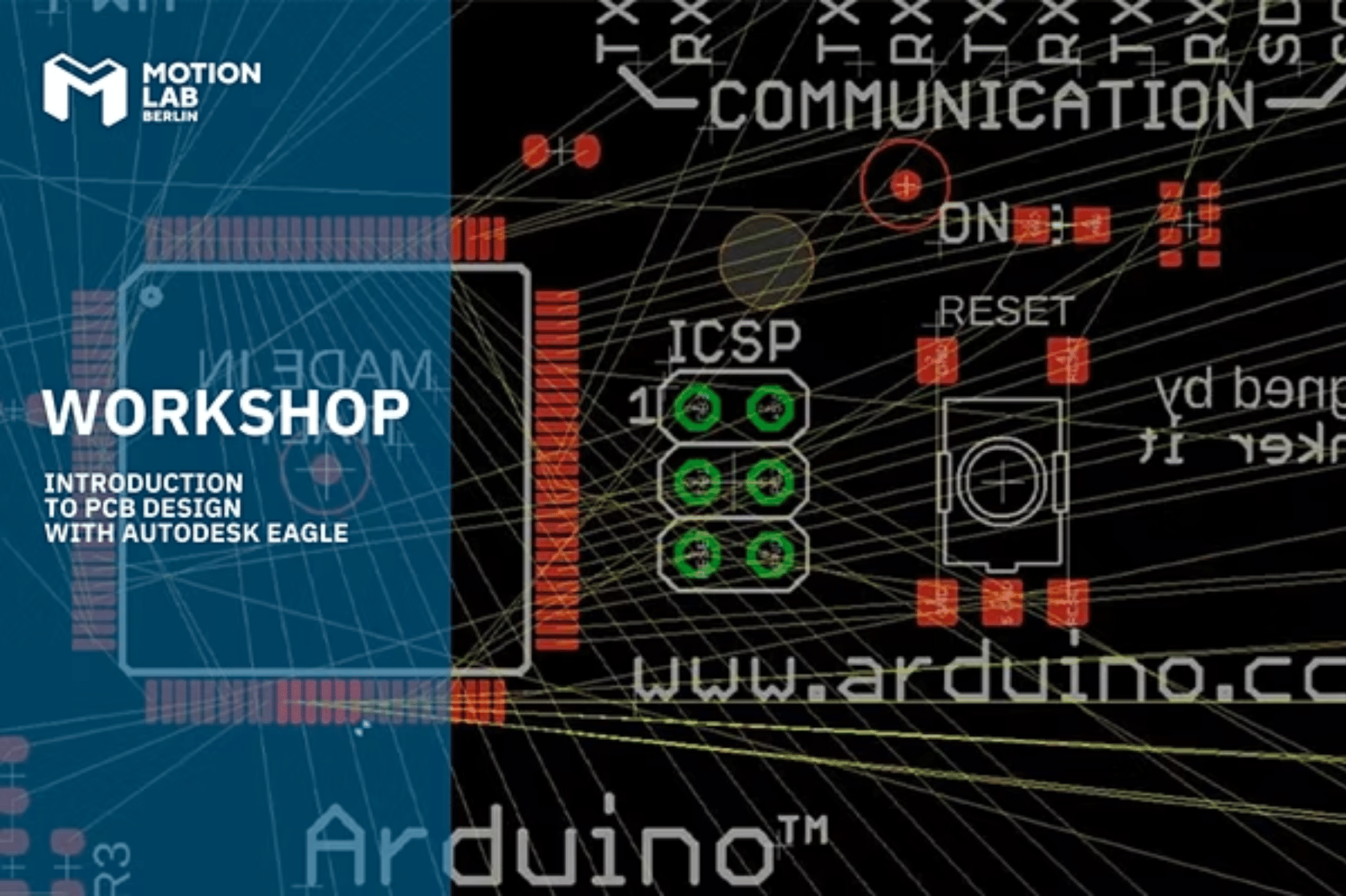
It will help you catch errors before the board is fabricated, and it'll help you debug a board when something doesn't work. Although it has no real effect on the circuit your designing, silkscreen can be a critical part of the PCB design. Some silkscreen -- like part outlines -- is automatically placed on the board because it's a piece of the part. We can manually add other information, like labels, logos, and names. A variety of draw tools -- wire (), text (), circle (), arc (), rectangle (), and polygon () -- can be used to draw on the silkscreen layer (tPlace for top, bPlace for bottom).
How to check your design for errors
There are many PCB designing software available in the market. You have to choose the software according to your budget, application, and knowledge. Here I have listed the most popular PCB designing tools; Eagle, Altium designer, Kicad, OrCAD, EasyEda, PADS, PCBworks, circuitmaker, etc. Hence, in this sequence of articles we will learn how to design PCB boards with Eagle Software. Keep in mind that DRC tolerances, such as minimum trace width and clearance between traces and components, can vary between manufacturers.
Adjusting the Dimension Layer
If two nets cross, but there's not a junction, those nets are not connected. The hard part, sometimes, is identifying which part on a circuit symbol is actually a pin. Usually they're recognizable by a thin, horizontal, red line off to the side of a part. Sometimes (not always) they're labeled with a pin number.
ECAD and MCAD: A Match Made in Fusion 360 - ENGINEERING.com
ECAD and MCAD: A Match Made in Fusion 360.
Posted: Wed, 28 Apr 2021 07:00:00 GMT [source]
Opening a Project and Explore
By default, this is set to be a much more fine 0.005". Then, starting at the origin, draw a box around your parts. Don't intersect the dimension layer with any holes, or they'll be cut off!
Schematic is a drawing which represents the circuit with component symbol and connection lines. In the schematic editor, add all components which is required by your circuit. After adding all components in the schematic editor, make a proper connection with wires. The board layout shows how PCB look like with actual size and place of components. There is a common button in the schematic window and board layout.

PCB layout, on the other hand, pertains to the placement of components on the PCB, the paths of connecting lines, and the spacing and arrangement of components. In the dropdown options for ‘Frame,’ locate ‘FRAME_A_L,’ double-click it, and the frame will move with the mouse cursor. If you need multiple frames, repeat the process, and you can quickly complete it by pressing the ‘ESC’ key on the keyboard. Organizing the placement of each component is crucial to the efficiency and size of each PCB. Remember that the larger your PCB, the more it will cost. Tracks between components should be as shortaspossible and as efficient as possible.
To adjust a part's value parameter, use the VALUE tool -- . The schematic layout is done, but there are a few tips and tricks we'd like to share before moving over to the PCB layout portion of the tutorial. Even though there's no green net connecting these pins, every net with the same, exact name is actually connected. To actually add a part from a library either select the part you want and click "OK", or double-click your part.
Additional Experience
To do this, just go ahead a click 'generate/switch to board' on the top bar. You should be able to see all the parts from the Adafruit library here. It is important to remember that because this is a schematic that will be used to make a PCB, the parts you choose do not have to be EXACTLY what you are looking for. However, the shape, dimensions and number of holes have to match.
Adjust Component Position
Running the SparkFun EAGLE script will get your UI to exactly match ours. Now, when you go back and look at the "Libraries" tree, there should be two folders included, one of which should be our SparkFun Eagle Libraries. The last step is to tell EAGLE that, for now at least, we don't want to use the default libraries. To do this, right click on the "lbr" folder, and select "Use none". Go to the "Options" menu and then select "Directories". This is a list of computer directories where EAGLE looks when it populates all six objects in the tree view...including libraries.
If you were trying to grab one of the other overlapping objects, right-click to cycle to the next part. EAGLE's status box, in the very bottom-left of the window, provides some helpful information when you're trying to select a part. Within EAGLE's board layout tool you create a finished PCB design. If you select a file in a tree, information about it will appear in the right-hand portion of the window.
Then (as usual), you'll need to adjust some settings in the options bar. Also adjust the Isolate setting which defines how much clearance the ground pour gives other signals, 0.012" for this is usually good. Support for OS/2 Presentation Manager was added with version 3.5 in April 1996. This version also introduced multi-window support with forward-/backward-annotation, user-definable copper areas, and a built-in programming language with ULPs. This UI setup presents a nice logical view of the layers.
EAGLE's board designer is where a good portion of the magic happens. It's here where the dimensions of the board come together, parts are arranged, and connected by copper traces. In the board editor, the conceptual, idealized schematic you've designed becomes a precisely dimensioned and routed PCB. The DIY electronics site SparkFun uses EAGLE and releases the EAGLE files for boards designed in-house.
If necessary, we can make minor modifications on-site. During the development process, we keep in touch with the industrial design studio to ensure that the enclosure and the board match each other. To do that, we will design a PCB and order electronic components. Our partners will manufacture the prototype and send it to us so that we can test it and amend it if necessary. We contact the customer to confirm the project requirements. Then, we create a technical specification and set a budget and deadlines.
The team tests the work of the board under corresponding operating conditions and runs some tests required for product certification. We get acquainted with the concept of the future device and sign a non-disclosure agreement. The team gathers project requirements, studies relevant documents, and analyzes rival products on the market. At this phase, a preliminary project evaluation is made.
EAGLE is far from the only PCB CAD software out there, and its design files are nothing like those of Orcad or Altium. Fab houses can't possibly support every piece of software out there, so we send them the gerber files instead. To place a via mid-route, first left-click in the black ether between pins to "glue" your trace down. Then you can either change the layer manually in the options bar up top, or click your middle mouse button to swap sides.


No comments:
Post a Comment